The Swirl Legacy
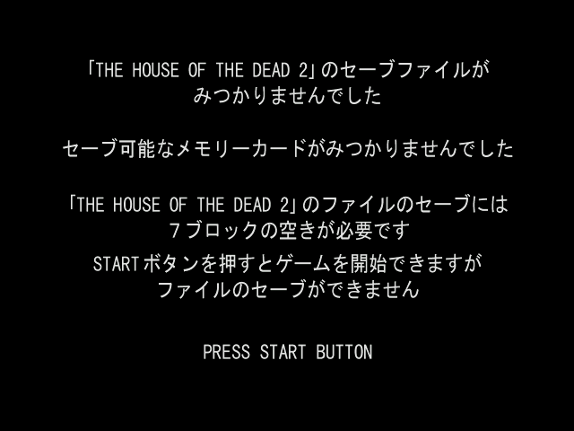
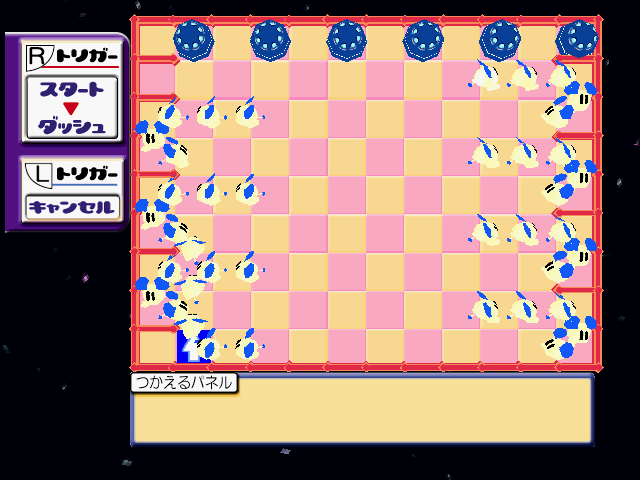
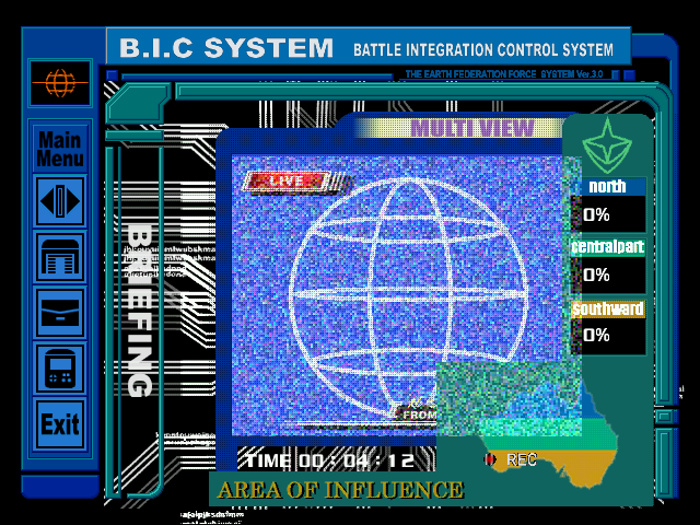
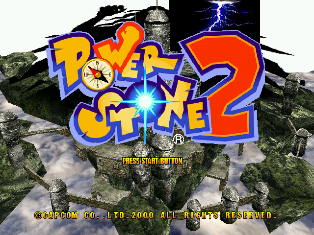
Fixed after two days of fierce coding/studying the code that prevented GD-ROMs to boot on Sega Dreamcast console. As usual with Sega, status flags are pretty picky on BIOS program …
Compatibility is pretty dire, as you might expect from a complex major system that has zero testing so far. No sound, inputs are mostly not working and several SCSI commands aren’t supported, but hey.
(EDIT: more pics)






August 26th, 2013 at 1:47 am
Hi, Kale,
I was sent a link to your good work on MESS / MAME, and wondered if you could help me?..
I’ve been trying to get my GDD emulator working on FPGA for many months now.
I recently abandoned the project as I could never get it to boot past the Sega license screen.
There’s quite a bit thread about the emulator on the AG forum…
http://www.assemblergames.com/forums/showthread.php?39733-quot-Let-s-make-GD-ROM-emulation-happen-quot-Facebook-group/page22
I also did a PCB design for a DC to IDE adapter, and that also only boots to either the license screen, or shows the “AICA_DRV -1″ error on the Crazy Taxi GDI. This would need to work with more of a software patch than a pure hardware solution like the FPGA.
Could you possibly provide any details on the status flags you needed to fix to get more GDI’s booting under MAME?
(All the FPGA stuff is done at a low level by loading the requested sectors directly from SD into SRAM, then streamed via DMA to the DC.)
I’ve tried many times to follow the SPI (Sega Packet Interface) manual, and the ATAPI spec to provide the correct flags, but it’s still not booting?
I haven’t properly implemented the FAD address info though, so maybe that is causing problems?
The FPGA isn’t big enough to make large captures via JTAG, so it’s almost impossible to log all the accesses and compare to a real GD disk.
Thanks for your work on this, the MESS / MAME effort is amazing. 😉
I look forward to your reply.
Please e-mail me if possible, as I do tend to type quite a lot.
OzOnE.
September 1st, 2013 at 5:45 pm
Uhm, lesse:
Most important status flags on GD-Rom are DRDY, BSY and DRQ, and I don’t think you need an explaination of what does what since that the manual already explains it well. “SAMTAG” (-> sense, register 0x8c) is also mandatory to make them to boot (I’m returning 0x81 here for now, GD-Rom detected + pause state, until I get bored and do the real deal + red book audio and MIL-CDs). If you don’t then the system goes in a “licensed by sega” -> “dashboard” loop. Also, US/EU systems needs the GD-Rom to be “unlocked” at 0x005f74e4 address. I haven’t yet determined what does what because Psyman actually told me to do that, might or might not be an important part in GD-Rom protection.
I still have to find a single game that bothers regarding FAD address, so that doesn’t seem to be an issue for the time being.
October 14th, 2013 at 12:52 pm
Ooops, sorry I took so long to reply. I forgot to keep checking back.
Thanks for the info. 😉
I’m usually setting 0x81 “GD_PAUSE” state on the FPGA as well, but I’m almost positive now that my boot issues are down to incorrect settings of the GDD flags…
There has been some great progress on the GD emu over on the thread…
cybdyn has managed to get his board booting GDI games. 😀
A few of his vids have been uploaded to YouTube…
http://www.youtube.com/watch?v=-IpuJR2-jSQ
I’m now working with cybdyn to hopefully get my version of the board working too.
We have been discussing the unlock stuff recently. I was wondering the same thing too – nobody seems to know exactly what gets “locked” before this register is used?
A few people have the IDE adapters now, and I started some of my first DC coding to attempt to get it to boot directly from CF card / HDD too (cybdyn’s FPGA project is a separate thing, and the only thing which is booting games on the real hardware so far, apart from Dreamshell)…
What I do know is that the register at 0x00574e4 needs the whole BIOS to be transferred “through” that register. Some sort of checksum algo is then done to determine whether it’s an unmodified retail BIOS or not.
That register is inside the HOLLY chip, so I’m fairly certain all the algo stuff is done on the chip itself. My theory is that it blocks the DMA transfers from the GD drive until this checksum is proved valid. Not sure about PIO transfers, as it’s fairly tricky to determine with my setup.
An emulator probably doesn’t have this reg ofc, so likely shouldn’t cause any problems.
I tried unlocking the drive access in my IDE adapter code, but it still only booted just past the license screen.
The FPGA version holds far more promise though, as we now know that booting games from it is working fine. A fair bit of work needs to be done to make it practical (TOC generation, image select menu, possible FAT32 traversing etc.), but it’s looking great so far.
I was wondering though – do you have a link to your most recent MAME WIP source, including these updates?
MAME has a fantastic debugger as you know (one of the best around), so would be good if I could use it to capture some more info on the boot process and flags.
Also, I’m assuming the GDI’s still need to be converted to a .CHD first?
Regards,
OzOnE.
October 14th, 2013 at 1:39 pm
Oh, just answered my own question about the NAOMI under Mame…
I just tried loading Jambo Safari, but it crashes.
Need to find if any of the ROMs are working atm, so I can do some debugging stuff…
After cybdyn’s success with the DC, I realized that it should in theory be easier to make a ROM / GD emu for the NAOMI instead. Thought I might as well branch off in that direction while cybdyn is working on the DC side.
I’ve already traced some of the G1 bus stuff on the real NAOMI board.
Most of it goes to the Altera FLEX FPGA ofc, but it should be possible to bypass that chip altogether.
The G1 data bus passes through the bus tranceiver IC’s on the underside of the board, so that part is easy to solder to. I need to find the rest of the control signals, but shouldn’t be too hard.
I bought a NAOMI last year, but it had it’s HOLLY chip removed by the previous owner (I was aware of this, but it was only £20, so I grabbed it anyway). This is actually quite handy ofc, as it lets me trace the signals quite easily.
As you very likely know, the NAOMI accesses the ROM pack or DIMM board via some simple offset regs in the FPGA (via the G1 bus), so I think it should be doable to emulate this on another FPGA.
Even better is if DMA pausing works as expected, as we can then store “chunks” of data in a small-ish SRAM, and just stream new data from SD card / HDD.
I’m now in the process of sourcing a working NAOMI, but the MAME debugger will be a fantastic help in the mean time. I know a very minimum amount of coding under MESS / MAME though, so was wondering if you’d be interested in helping with the occasional question?
Please e-mail me if you get chance, be good to talk about this some more. 😉
Best regards,
OzOnE.